When medical devices fail, patients can suffer. So every effort must be made to ensure the devices operate as planned during their entire service lives. To that end, IPC provides several relevant standards documents that dictate design decisions for high-quality, high-reliability PCBs. These IPC recommendations, requirements, and suggestions are separate from safety requirements mandated by regulatory agencies.
Class 3 Fabrication / Assembly
for Class 3 fabrication on every board produced. However, manufacturing is inherently variable, and machine operators have different experience and skill levels, so no two boards are identical. Boards that do not meet Class 3 specifications either go to rework or to a landfill. PCB designers should use best practices in their board designs to maintain a high yield that allows for slight variability during manufacturing.
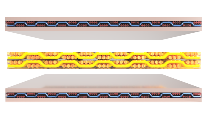
Vias
for interior-layer vias. The problem is that copper is a tough material and drills can wander as they progress through layers. Additionally, layers shift during the lamination process. To solve
this problem, manufacturers add a few mils to their minimum pad size to account for manufacturing variability that still allows the part to meet Class 3 specifications. Customers with boards that are on the lower edge of allowable pad size might opt for machine-vision-assisted mechanical drill centering, a less-commonly available option.
stack and laser-drilled vias on the outer layers.
minimums when possible.
Solder Dams & IPC-7093 Land Pattern Design
Vias placed in pads or so near to pads that there is insufficient room to either tent or create a solder-mask dam at least two mils wide, will wick solder away from a joint during reflow. And with insufficient solder present to meet Class 3 inspection criteria, both yield and reliability will decrease, while rework expenses will increase.
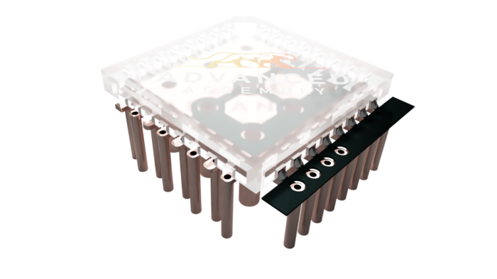
This image of a 32-pin QFN package has vias in and near pads (left) that will wick solder away from the pad and leave an unreliable or failed joint. On the right, soldermask creates a small dam to prevent solder from flowing into the open or tented vias.
Sometimes engineers have no choice but to place a via-in-pad in very tight-pitched BGA designs, and in those cases, they should factor the cost of Via-In-Pad-Plated-Over (VIPPO) processing into the final budget for their design. But for a mission-critical device that cannot tolerate failure, vias should be moved several mils away from a solder pad and tented or dammed to prevent solder from moving into the via cavity during reflow. Engineers can do this with a traditional dog-bone BGA breakout pattern in a wagon-wheel or similar pattern.
High Currents & Heavy Copper
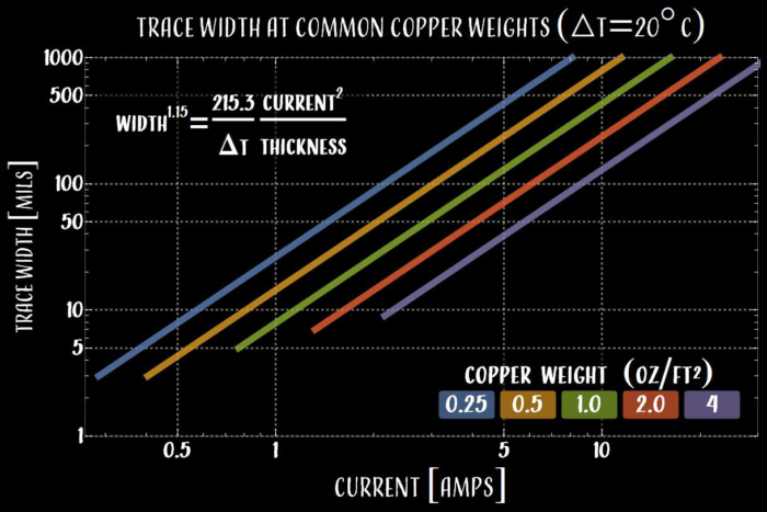
volume of copper can dissipate heat through conduction, convection, and radiation. Unfortunately, many medical device designers rely on the tables and trace-width calculators based on the now deprecated and far too conservative IPC-2221 standard. IPC-2152 has since replaced IPC-2221 and provides for much smaller trace width and copper weights. But even the new standard is more conservative than necessary since it assumes a single isolated trace and neglects all of the other copper on a PCB that might act as a heat sink in the design.
Low EMI Design
machines. With all of the intentional radiators in the space, it is essential to limit unintended emissions caused by poor layout practices.
the critical understanding of the underlying concepts of conduction and displacement currents. Students tend to view a “ground plane” as the universal return path that all signals take. While that might be a designer’s intended return path, there are no laws of physics that preclude any other nearby conductor from becoming the return path for a given trace.
speed of causation (speed of light) in the surrounding medium.

With a minimal signal transition time, the propagating electric field energy gradient is high and causes charges to accelerate when the disturbance encounters nearby conductors. The easiest way to mitigate the effect is to slow the signal transition speed wherever data transmission rates allow.
Close Coupling
There are two common ways to create a PCB, termed “foil” and “cap” construction. In foil (also known as sequential) construction, fabricators start with a single copper-clad central core and progressively add layers of prepreg and foil to create the final design.
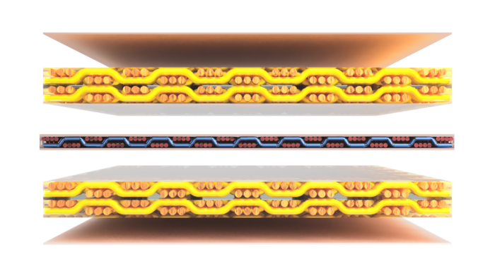
In “cap” construction, fabricators start with several copper-clad cores and sandwich prepreg between the various cores.
The fabrication methods and the stackup specifications create conduction layers with various thicknesses of dielectric separating them.
For best results, route return paths on a copper conductor immediately adjacent to the signal layer. Never route a high-speed return path through a conductor to a non-adjacent layer. In a six-layer board with a signal on layer two, possible return paths are layer one and layer three, and whichever layer is physically closest to layer two is the preferred choice. But the signal return
will follow the lowest impedance path. You should never route a return for layer two on layer four unless there is a copper void on layer three. Electromagnetic fields will not couple to a far away
conductor by coupling through a nearby conductor — they will simply couple to the nearby conductor.
Routing Vertical Returns
Routing a PCB is like playing an advanced version of the computer game “snake,” every routed trace makes it more difficult to route the next. Eventually, single-layer routing becomes impossible, and an engineer must shift the net to another layer to avoid colliding with other nets. Even engineers who know how to route return paths on adjacent nets often forget to create a low impedance vertical return path between their current and new layers. Without at least one dedicated return via, the intended return path will be non-continuous, forcing the energy to either find a return path the engineer didn’t imagine or radiate out into the environment.

Going Further
Signal integrity and long-term device reliability are two of the most critical design considerations for medical device manufacturers. Numerous layout best practices can ensure that your product will pass electromagnetic emissions and compatibility testing. To learn more about design best practices, look into the work and writing of experts in the field such as Eric Bogatin, Rick Hartley, and Stephen Hall, etc. Here are a few selected resources.
• “Signal and Power Integrity — Simplified” — Eric Bogatin, 2009
• “Advanced Signal Integrity for High-Speed Digital Designs” —
Stephen H. Hall, 2009
• “Right the First Time: A Practical Handbook on High Speed
PCB Systems Design” — Lee Ritchey
• “High Speed Digital Design: A Handbook of Black Magic” —
Howard Johnson, 1993