Since working with HDI boards can be challenging, our engineers have created a white paper to help ensure that your designs work the first time. 

High-Density Circuit Boards

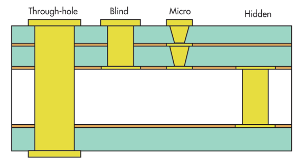
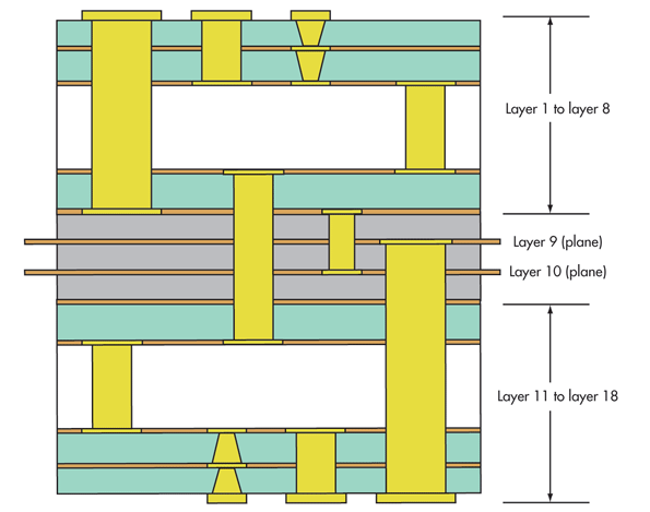
Due to the growing complexity of design structures, high-density circuit boards (HDI) are being used more and more, especially in consumer electronic products. As products increase in functionality and decrease in size and weight, circuit board engineers need new solutions to maximize space on each board. Blind and buried vias and vias-in-pad add complexity to the design, but let you do more with less. Royal Circuits focuses on these advanced technologies.

HDI technology gives designers more space on their PCBs to place smaller components even closer together. Types of HDI PCBs include:

  • through vias from surface to surface
  • buried vias with through vias
  • two or more HDI layers with through vias
  • and passive substrate with no electrical connection

PCB vias come in different configurations:

  • Through-hole (TH) vias originate and terminate at the outer layers of the PCB
  • Blind vias originate on an outer layer and terminate on an inner layer
  • Buried vias are completely buried within the board, connecting only inner layers and not reaching the outer layers at all
  • Microvias are a form of blind vias that penetrate only one or two layers, and they have an extremely small drill hole​

Below are a few images that illustrate different types of vias

Vias come in different configurations including through-hole, blind, micro, and hidden.

Multilayer boards can incorporate different types of vias to minimize the number of layers required.