Curing ovens are an integral part of any Printed Circuit Board (PCB) manufacturing and assembly industry. The market offers a huge range of standard and custom-made ovens for composite curing, both in-line and bench-top types. Typically, these ovens provide a unilateral flow of air that delivers heated air from two sides of the chamber to create a uniform operating temperature within.
Manufacturing multilayer PCBs involves sandwiching the Prepreg between very thin and loose sheets of copper and the inner core. Under pressure and heat in the curing oven, the Prepreg flows and binds the layers together. The assembly has to cool to room temperature before further processing commences.
The choice of a suitable oven for PCB curing depends on several factors such as:
- Type of PCB under production—whether glass epoxy, Polyimide, or others
- Production capacity—decides the size of the chamber, conveyor, and airflow
- Temperature requirements
- Design and construction requirements
- Special processing needs
- Control capability needs
- Selection between standard and custom configurations
Disadvantages of Curing with Hot Air
Depending on the Prepreg the fabricator is using, the oven must reach a specific temperature before the actual chemical reaction for bonding can take place. The curing oven raises the temperature of the ingredients to a specified level and maintains this temperature for a set time. Typically, conventional heat ovens take about 90 minutes to complete the curing process. Of late, there are attempts to reduce the curing time.
Another disadvantage in using hot air is its oxygen content encourages oxidation and creates air bubbles. Preventing this requires a nitrogen purge, which adds to the complexity and cost.
Using Super-Heated Steam in Curing Ovens
A significant improvement is to use steam rather than air to deliver the heat in the oven. While the specific heat of air is 1.01 kJ/kg, it is 1.97 kJ/kg for high pressure steam. That means steam at high pressure can deliver nearly twice as much heat than hot air can at the same temperature. This not only cuts down the curing time, the total energy consumption for the curing process is much lower than that of a conventional oven. Moreover, as hot steam is essentially water and does not introduce oxygen, it also eliminates the need for a nitrogen purge.
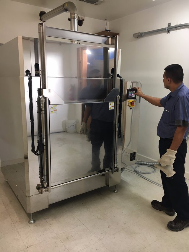
A typical steam curing oven comprises an oven housing, the housing flues, the steam generator, fans, and the steam regulating mechanism. Initially, as the steam generator produces the steam, it is in the form of a white mist—a mixture of vapor molecules and water particles—known as wet saturated steam.
The wet saturated steam then passes through an infrared or microwave heater, which heats it further, vaporizing all the water content to create dry saturated steam. Although the steam at this point does not contain water vapor, its temperature is still at 100°C, the boiling temperature of water.
Additional heating raises the temperature of the dry saturated steam to beyond 100°C, making it superheated. At this time, the steam is made up entirely of nanoscale molecular particles with an average diameter of 0.4 nm. In the industry this type of steam is also known as nanosteam.
Inside the curing oven, a mixture of compressed nanosteam and high-pressure air is sprayed onto the PCB sandwich, causing the Prepreg to flow rapidly.
Advantages of Using Nanosteam

While hot air simply heats up the surface of the material, the super-energized tiny particles of nanosteam easily penetrate a large mass, delivering their heat to the innermost reaches. This allows most of the Prepreg to reach the required curing temperature must faster and more evenly. The result is the time taken for curing reduces drastically. For instance, where conventional curing oven take approximately 90 minutes to complete the process, a nanosteam curing oven cures the PCB assembly in only 10 minutes—improving the throughput, decreasing power requirements, and reducing cost.
Using nanosteam for bonding Prepreg and copper laminates has the advantage of preventing voids at the interface. Void formation during curing can affect critical performance metrics such as bond strength, thermal transfer, and stress decoupling, which can ultimately lead to poor reliability of the PCB. As voids are pockets of air trapped during the lamination process, the void content tends to increase with increasing path lengths of air escape. Uniform heating of the Prepreg and the copper laminate with nanosteam does not allow voids to form, improving the PCB reliability.
Not only for curing PCB laminates, nanosteam ovens can also cut down the time required for curing legend printing on PCBs as well. Curing time for legend print in conventional heat ovens can take up to 60 minutes, but a nanosteam oven can cure the same more uniformly in only 5 minutes.
The high efficacy of nanosteam in curing and drying a substance comes from its dual action. As nanosteam particles penetrate deep into the substance mass, they release heat to the inner regions and raise the internal temperature of the substance so it starts to dry from the inside out. At the same time, the hot steam also dries the surface of the substance driving the heat from the outside to the inside. In conventional ovens the hot air does not penetrate deep under the surface.
This can cause the surface of the substance to dry out faster than its inner core does, thereby allowing a shell or a crust to form. Hot gases trying to escape from the insides lift these shell/crust in places to form blisters. If the internal pressure increases further, the blister may burst or puncture, leaving the entire surface pitted. For instance, blisters can burst sending solder mask into unwanted areas.
Optimized drying using nanosteam causes very even drying throughout the substance, preventing the formation of voids, crusts, shells, blisters and the like, and the result is a uniform surface free from blemishes.
As with other types of ovens, thermal profiling is also an important factor in nanosteam ovens. This is more so as the curing time in nanosteam ovens is much faster. Therefore, the ramp-up times and cooling-down times need to be adjusted more finely than in conventional ovens.
Stored PCBs generally tend to absorb moisture from the atmosphere, which can lead to reliability issues when assembling them with SMD components. The issue is tackled by baking the PCBs inside an oven at an elevated temperature for a certain duration. Stacking PCBs one on top of another complicates the baking process, as heat is unable to penetrate to the inner PCBs.
Baking the PCBs in a nanosteam oven overcomes the uneven heating, as the nano particles of superheated steam penetrate deep into the stack of PCBs. This allows even the PCB at the middle of the stack to heat up uniformly and release its moisture quickly. The result is a faster and more efficient baking process, while the power consumption reduces.
Future Progress
A wide range of industrial and commercial processes use steam in normal and superheated form. However, generating nanosteam requires vast amounts of energy, reducing the overall efficiency of the process. This is leading scientists to look for shortcuts—producing steam without expending too much energy,
By suspending light-absorbing nanoparticles in water, researchers at Rice University are able to turn water molecules around the nanoparticles into steam while the remaining water retains its lower temperature. Therefore, using light, it is possible to generate steam without raising the temperature of water. Once commercialized, the technology can reduce the cost of many steam-reliant processes drastically.