Designing a Layer Stack

What is a Stackup?

PCBs are made of alternating layers of conductors and insulators (dielectrics). 

Multi-layer PCBs are either made by laminating two or more premade cores together, or by starting with a core and laminating foil on the outside to build up the outer layers.

This image can be seen in two ways. It either shows two 2-layer cores (black) with prepreg (white) joining them together. Or it could be a single 2-layer core (white) with copper foil attached with prepreg (black).

The conductor for rigid PCBs is almost always copper.  Occasionally you will hear about aluminum in the middle of the board, but it usually is there to act as a thermal conductor, not an electrical conductor.  The insulators are made of a variety of materials that range from inexpensive and easy to work with fiberglass to expensive and hard-to-fabricate Teflon (for RF designs.)  

The copper layers are counted from the top to the bottom and referred to by their layer number: “Layer 1”, “Layer 2”, etc… Often, you’ll hear the layers referred to as other things, including “inner-layer”, “outer-layers”, “plane-layer”, “signal-layer”, “top-layer”, “bottom-layer”.  

2. Symmetry

A general rule for designing a core stack is to ensure that it is symmetrical about the middle.  

This eight layer rigid-flex design has two layers of flex with two additional layers laminated to either side.

If your stack is not symmetric, differential coefficients of thermal expansion will likely cause the board to warp during assembly and operation.  This is primarily a problem on very thin PCBs.  Copper acts to constrain the expansion in places & directions where it is present but does very little to constrain expansion in lateral directions.

This type of warpage is caused by uneven copper etching on opposite sides of a core.
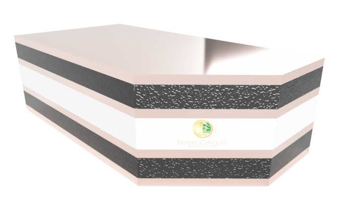
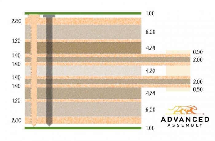
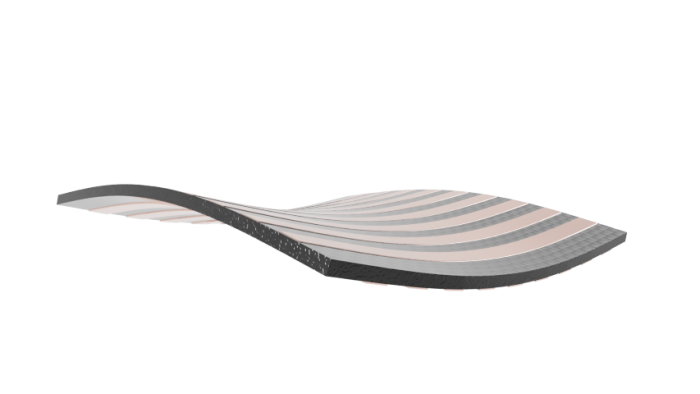
"Most engineers know that they need to design a balanced layer stack to prevent warpage during assembly. But it's pretty often the case that engineers will remove large amounts of copper during the routing process resulting in an unbalanced stackup. If you don't keep track of your copper symmetry, you will end up designing a potato chip."
Mark Hughes
Designer

Recent Posts

Summit Interconnect Acquires Royal Circuit Solutions and Affiliates

The combination solidifies Summit’s position as one of the largest privately owned printed circuit board (PCB) manufacturers in North America with a  footprint that will now encompass eight manufacturing facilities. The acquisition significantly broadens the scope of Summit’s product offering while expanding the company’s business portfolio of key customers and end-markets. Summit Interconnect is pleased… View Article
Read More

Tech Chat with Thermal Expert, Mike Jouppi

Ever wondered how many vias to use in a thermal package? Or how to route high current traces in small spaces? Good news! Mike Jouppi is back! Check back for a recording of this important PCB resource. In the meantime, feel free to download the Thermal Resistance calculator discussed live.  Download Thermal Resistance Calculator
Read More

Flex PCBS: Design Tips and Material Selection Advice – On-Demand Webinar

In today’s high-tech world, electrical engineers have many choices when it comes to designing their PCBs, including what type of laminate to use. Laminates form the foundation for a high-functioning PCB. In this on-demand webinar, learn how to select the right laminate for your project based on material properties, suppliers, types and more.
Read More

Share

Share on twitter
Share on pinterest
Share on facebook
Or use this public share link