Why is Pulse Plating Better?
Manufacturers have traditionally used acid copper for direct current electroplating of copper tracks, vias, and through-holes on their Printed Circuit Boards (PCBs) with copper. Although direct current electroplating offers high leveling and bright covering power, this method suffers from poor throwing power. With PCBs increasing in density and complexity such as reduced via diameters, excessive plating times are necessary to achieve minimal copper thickness in low-current-density areas.
Problems with DC Electroplating
With direct current electroplating, the problem manufacturers face is in controlling the amount of copper inside the holes. The hole diameter reduces with the progress of plating, as the number of metal layers necessary to complete the plating through the hole increases. For instance, for a 1 mil coating at the center of the hole, the amount of copper necessary on the surface of the panel is at least two to three times more than the regular thickness. It also means the entire plating time would take two to three hours longer to complete.
Some manufacturers tried to solve the problem by dual rectification where they used two electrodes on either side of the PCB. Although this did help to cut down the total plating time, it did not solve the problem of uneven plating thickness. Lowering the current density was one way of equalizing the copper thickness over the surface and in the through holes and vias, but this prolonged the process duration such that it practically negated any advantage dual rectification offered.
Pulse Plating Technology
In its most basic form, pulse plating technology uses a pulse rectifier that converts Alternating Current (AC) into a Direct Current (DC) pulse train with regular cycles of rectangular pulses for the electroplating process. In each cycle, the pulse rectifier allows DC voltage output for a certain duration and blocks it for the rest of the duration, with the ratio of the on time to the cycle time being the duty cycle. Although initially the duty cycle was a constant, people soon realized they were able to achieve better results with a duty cycle they could adjust depending on the plating process. Therefore, with a 100% duty cycle, the electroplating process could use a continuous DC output as the earlier process did.
Such pulsing DC voltage output, at less than 100% duty cycle, produces a modulating current. The plating process under such modulating currents is called modulation current plating and it plays a significant role in the quality of plated coating. For instance, the pulse plating current may be significantly higher than that in the direct current plating method, but the former offers a more detailed crystalline coating. The reason is the high instantaneous periodic current density reduces the high potential of metal ions such that the deposit is a layer with fine grains.
Reverse Pulse Plating Technology

Of late, a newer product by the name of reverse pulse rectifier is available in the market. Besides delivering the normal forward pulse, the reverse pulse rectifier also delivers a reverse polarity pulse within each cycle. In simpler reverse pulse plating rectifiers, although it is possible to adjust the individual time periods of the positive and reverse polarity pulses, it is not possible to adjust their amplitudes individually.
More advanced reverse pulse rectifiers are also available, where the user can adjust forward pulse amplitude as well as the reverse pulse amplitude individually. This depends on the actual chemical process, and for pulse plating applications in the PCB industry, it is sometimes necessary to adjust the reverse pulse amplitude up to three times the amplitude of the positive pulse. However, as the duration of the reverse pulse required is only 2.5-10% of the duration of the forward pulse, the power delivery requirement from the reverse pulse rectifier is not substantially different from that required from a regular pulse rectifier.
Advantages of Pulse Plating
Complex PCBs may have a wide variety of hole diameters along with other special properties. For plating such boards effectively, it is necessary to adjust the amplitudes as well as the time periods of the forward and reverse pulses during the plating process. These adjustments ensure the best performance of the plating process, as the parameters depend on specific properties of the board. The user typically works with a batch program, adjusting one or more amplitudes and time periods to obtain the best results.
In practice, there is very little difference in the electro-chemical process for direct current, pulse, and reverse pulse acid plating—the difference is mainly visual. While not required for direct current acid plating, operating parameters for pulse and reverse pulse rectifiers are under computer control. The advantage is the user can pre-program all work practices and batch files. Just as in traditional acid copper plating, it is usual for pulse plating and reverse pulse plating systems to also use brighteners, carriers, and water additives to improve the plating efficiency.
The pulse plating method produces desorption of the special additives when the current density crosses a specific threshold. Desorption is the process by which a chemical retains its mobile phase, rather than sticking to its stationary phase, and this results in increased reaction from the chemical. In practice, desorption enhances the resistance in the areas where high current density exists, thereby increasing the throwing power of the electrolyte, resulting in more even plating thickness. The reverse pulse plating method enhances this effect even further.
A further advantage of the pulse and reverse pulse plating methods is they can use lower concentrations of copper metal in the electrolyte, thereby reducing the amount of sludge the plating process generates. As both pulse plating processes improve the throwing power of the electrolyte into areas with low current density, they require less time for generating a minimum copper thickness. The advantages of reverse pulse plating are:
Metallurgical Advantages
- Deposits are denser
- Porosity is lower
- Deposit grains are finer
- Tensile strength of plating is higher
- Plating has higher elongation capabilities
- Stress on the PCB is lower
- Hydrogen embrittlement is lower
Physical Advantages
- Plating adhesion is better
- Throwing power of the solution is higher
- Plating thickness is more uniform
- Hole-wall thickness is more uniform
Electrical Advantages
- Plating has higher conductivity
- Plating has lower resistance
- Bond-ability of plating is superior
General Advantages
- Process limitations are lower
- Better control of metal content in bath
- Lower requirements of additives
- Plating time or process time reduces
Special Requirements for Pulse Plating
As pulse plating systems use high current waveforms with square pulses, low inductance cabling helps to preserve the sharp rise and fall times. In general, the industry uses twisted welding cable or coaxial cables. Moreover, as the pulse plating process consumes additives at a higher rate than conventional DC acid plating processes do, it is usual to have a tank with weir.
As the pulse plating process uses higher current densities compared to regular DC plating, using air agitation helps improve the efficiency of the process.
The Process of Electroplating
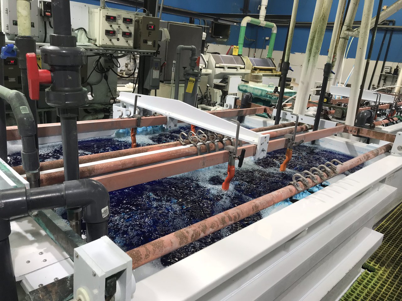
While electroplating PCBs, an electrochemical process deposits a metallic coating of copper on the traces and in the holes of the PCB, when it is immersed in a plating solution and a low voltage electric current passed through the solution. The PCB to be plated forms the cathode, linked to the negative terminal of the power supply, while a copper plate forms the anode, linked to the positive terminal. The electrolyte is a salt solution of copper, submerging the anode and the cathode.
Passing current though the solution causes the electrons in it to circulate through the battery and accumulate on the cathode. This attracts the positive ions of copper in the solution to the cathode. Since the PCB to be plated is the negative electrode, positive metallic ions accumulate on it to produce the desired copper plating. Quality of the plating on the PCB depends to a large extent on the current flowing in the electroplating process. The amount of current flow decides the thickness of the tracks, its structure, and the overall time for the plating.
Current flow in electroplating may be in the range of 100 to 2000 Arms. Tracks on a PCB are often larger than the through-holes, and this makes it difficult to ensure a uniform copper deposit. Typically, copper ions accumulate at places where the current density is higher, such as on the edges of holes. That also means they avoid places with low current densities such as deep inside through-holes. The net result is a higher deposit of copper on the edges of the holes compared to within the holes.
The situation improves by using a lower current density, but that leads to a longer process time. In addition, low current density results in deposit of coarse copper inside the hole, leading to cracking in the hole wall.
Quality in Reverse Pulse Plating
Reverse pulse plating using an appropriate electrolyte gives much better results. The reverse current forms a shield on the sensitive areas such as the edges of through holes. The positive pulse causes the shield to disappear progressively from the protected areas as the deposit begins on the unshielded areas. This causes a lower deposit on the sensitive areas as compared to the others. The process ensures a deposit of uniform thickness of copper through the holes and at their edges.
For the best quality of plating, it is necessary to ensure the pulse current waveform stays stable and unchanging with load. If there are undershoots or overshoots in each pulse, they need to be compensated. The quality of plating also depends extensively on the rise and fall times of both the forward and reverse pulse currents.
Reverse pulse plating systems with closed loop control use current transducers to allow continuous monitoring and adjustment of the current pulse waveforms. Typically, such systems provide quick response times of less than 1 µs at 90% of the nominal current. This allows a real-time control of the rise and fall times of the current pulses in the system. Other systems may allow bipolar AC and DC current measurement, bipolar DC power supplies, galvanic isolation, and EN 50178 compliance.
Proper current levels and pulse timings are essential for exact results of high-performance coatings on PCBs. Proper settings ensure production of pore-free, denser, and corrosion-stable layers. The pulse plating process ensures the plating is extremely uniform, even when the PCB geometry is complex.
With reverse plating process, the total time to process is reduced, which increases the system throughput. As the layer thickness is more uniform, expensive materials such as copper consumption reduces significantly. Additionally, mechanical post-processing also reduces significantly.
Conclusion
Reverse pulse plating technology has proven its advantages not only in the PCB industry, but also in numerous demanding applications. For instance, it provides high-performance functional and more exact decorative coatings for aerospace. In combination with dispersion coating techniques, reverse pulse plating technology can improve specific properties such as hardness.