Adding the Raspberry Pi Pico to Your Next Project

The latest toy in the electrical engineer’s toolbox is the Raspberry Pi Pico, a $4 microcontroller module.  The module hosts the bespoke RP2040 integrated circuit — the first completely custom silicon from Raspberry Pi.  And now that they’ve got that skillset on their resume, I’m sure we can expect some interesting iterations of the next Raspberry Pi computer and computer modules.  But today’s problem-to-be-solved is how to incorporate the Pico into your next prototype design-build.  And for that, it’s worth noting where they got their footprint.

Image of the Raspberry Pi Pico board from Raspberry Pi Pico Datasheet

Adafruit Feather

Adafruit Industries is a New York based company owned and operated by Limor “LadyAda” Fried.  Adafruit makes or distributes all the toys, trinkets, and tools that budding schoolchildren, makers, hackers, and practicing engineers need in their toolbox to make their projects “go brrr.”  And perhaps more importantly, they back it all up with educational tools in the way of tutorials, documented code, videos, etc… Between Adafruit and Sparkfun, there’s enough quality content there to constitute a complete undergraduate education in electronics and computer engineering.  A lot of engineers know about Adafruit (and SparkFun), and those that don’t, likely should.

Image of Adafruit Feather boards from learn.adafruit.com

It’s quite a neat little ecosystem, complete with a variety of ISM-band radio systems, microcontroller hosts, graphic displays, motor controllers, sensors, etc…   There are quite literally hundreds of “wings” and accessories that will work together.

The Raspberry Pi Pico Thing Plus

The engineers over at Adafruit obviously thought enough of the pico design to base their Thing Plus Raspberry Pi Pico layout on the feather footprint since the 0.1” pitch PTH line up with the feathers perfectly. This should make it very easy to get some prototypes up and running quickly.  In fact, if you are wondering how engineers have created advanced prototypes for a module that hasn’t even been on the market a week yet, it’s because they have taken another design and simply replaced the microprocessor module.  

The Raspberry Pi Pico Module

The Raspberry Pi crew went one step beyond the original footprint and added castellated vias for surface mount compatibility.  And if you want to use the Pico in your next design, the most cost-saving design decision you can make is to use a surface mount footprint. 

For that, the datasheet provides the following land pattern recommendation. 

Land pattern is taken from the Raspberry Pico Datasheet

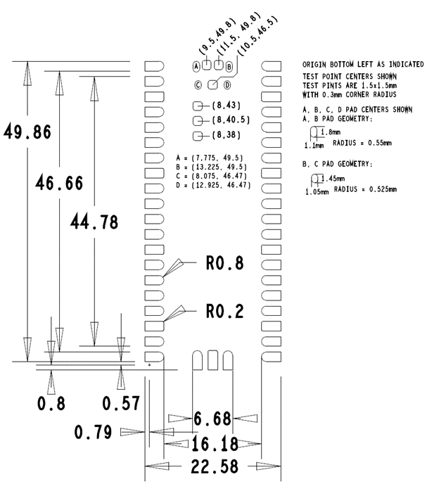
You’ll note that the dimensions are all given in metric measurements of millimeters, and only some of the pads are referenced to a particular datum.  The rest of the points are provided as relative measurements, which is unfortunate since most introductory EDA program still locate things on a cartesian coordinate system with pad centers referenced to a datum, not to each other.  Higher-end software packages have IPC-735x footprint generators that can work with the relative measurements, but none of the five EDAs I have available to me can deal with that particular footprint by means of a generator. 

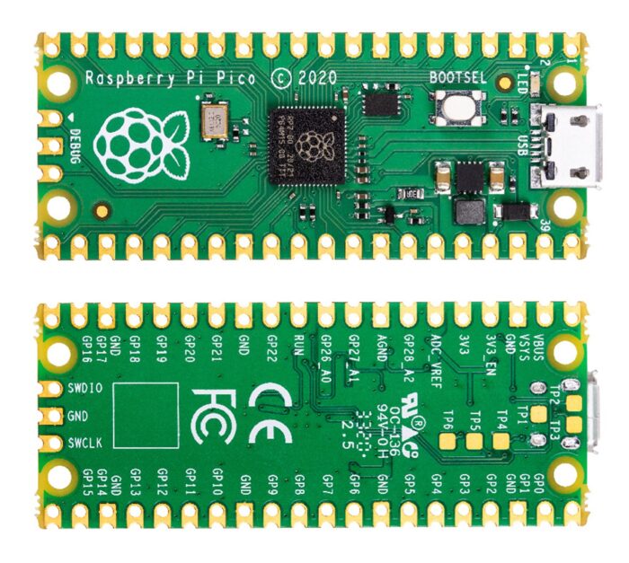
But don’t let those mean metric measurements make you feel all icky inside dear reader.  The pads along both edges are spaced 0.1” (2.54 mm) on center.  They are 1.6 mm tall, 0.79 mm wide, and the air-gap between them is 0.94 mm. 

The test pads appear identical in size to the USB interface pads.  They don’t appear to match the dimensional drawings given on the right side of the page at all.  For some reason, pad D seems to have been snapped from existence — perhaps the designers realized that the differential data pair only needed a ground return and not a VBus connection.  Either way, I suspect the data on the right side of the diagram is left behind from a previous spin of the board.  Oh, those jokers!

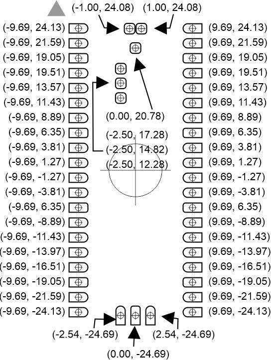
If you move all of the measurements so that the center of the pad nearest the original datum is (0 mm, 0 mm), and measure everything from there, it gets a whole lot easier to see how to put the land pattern into your EDA library editor.  But it’s still not ideal, there’s no pin 1 indicator, and the choice of the (0,0) point is still rather arbitrary.

This image shows the center location of each land pattern smt pad as measured from the center of the lower-left pad. Innermost pad sizes in this image are not to the specification in the datasheet and should be interpreted for illustration only.

But, wait!

If you make the part, you might as well have (0,0) close to mid-x and mid-y of the part, nowhere near that lower-left corner datum where the cartesian coordinate (0, 0) used in the original image is located.  Pin one, indicated by the large triangle near point (-9.69, 24.13) should also be indicated on your land pattern.

But what about the test-point and USB pads?

If you aren’t going to use the pads in your design, the datasheet recommends a copper void directly underneath them.  Although, as long as you ensure there is soldermask between the pad and any copper on your board, you should be fine.  If you are going to use them, you might consider a solder mask defined pad that is at most 1.5mm x 1.5 mm.  Or at least that should work until a datasheet correction is issued.

Recent Posts

Summit Interconnect Acquires Royal Circuit Solutions and Affiliates

The combination solidifies Summit’s position as one of the largest privately owned printed circuit board (PCB) manufacturers in North America with a  footprint that will now encompass eight manufacturing facilities. The acquisition significantly broadens the scope of Summit’s product offering while expanding the company’s business portfolio of key customers and end-markets. Summit Interconnect is pleased… View Article
Read More

Tech Chat with Thermal Expert, Mike Jouppi

Ever wondered how many vias to use in a thermal package? Or how to route high current traces in small spaces? Good news! Mike Jouppi is back! Check back for a recording of this important PCB resource. In the meantime, feel free to download the Thermal Resistance calculator discussed live.  Download Thermal Resistance Calculator
Read More

Flex PCBS: Design Tips and Material Selection Advice – On-Demand Webinar

In today’s high-tech world, electrical engineers have many choices when it comes to designing their PCBs, including what type of laminate to use. Laminates form the foundation for a high-functioning PCB. In this on-demand webinar, learn how to select the right laminate for your project based on material properties, suppliers, types and more.
Read More

Share

Share on twitter
Share on pinterest
Share on facebook
Or use this public share link