Introduction
Civil Engineers have a saying: “Any idiot can
build a bridge that stands. It takes an
engineer to make a bridge that can barely stand.” To achieve their goals, Engineers have finite
element and lumped element analysis available to them that allows them to
simulate all manner of loading and failure analysis. With that safety information in hand, they
can make decisions to decrease cost. The
technical aspects are specific to the field of Civil Engineering, but the
processes are universal to all disciplines – make it work, make it safe, and
then make it inexpensive. Engineering is
at its heart, a compromise between competing requirements and risk, with cost
and safety usually winning the day.
The same idea can be applied to PCB
design. While not every idiot can build
a HDI PCB, “It takes an engineer to make
an HDI PCB that barely works.” That is
because the “barely” can come with significant cost savings. You can absolutely go out and purchase
Roger’s core material, use 2 oz. copper, and have a design that works. But can you replace iTera MT40 with 1080 FR4,
and the 2 oz. with 1 oz. copper? You
will never know until you either simulate your design or take the chance of building
your board with less expensive materials.
The purpose of this article is to convince your company to invest in the
tools you need to do your job so you can purchase less expensive materials from
us, and make your overall design less expensive to produce.
The operating frequency of your design
isn’t all that important. In your
decision to simulate or your selection of test equipment, the critical number
you need to pay attention to is the rise-time / fall time of your fastest
signal in your circuit.
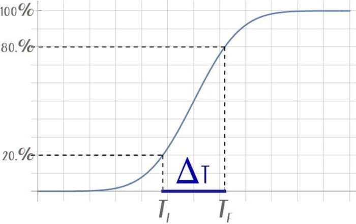
This time-domain graph shows the potential difference on a hypothetical trace during a logic transition from low to high. Rise time is measured as the interval between 20% and 80% of the logic-high voltage or the 10% and 90% interval.
It is possible (although unlikely) to have a leisurely 40 kHz switching frequency with a 20 GHz equivalent rise time by using a fast GaN switch. Frequency is the reciprocal of the period, so 1/50 ps = 20 GHz (20 GHz is an approximation since the choice of 80/20 or 90/10 is somewhat arbitrary and I’m ignoring a few other details.) To reiterate — you might be designing a “low-speed” circuit on paper, but in practice, it could be a very, very high-speed design. And those high-speed harmonics, reflections, etc… might completely disrupt your design.
And to make matters worse, it’s not just the fundamental frequency (determined from rise-time) that you need to worry about. In the frequency domain, square waves are made of a series of lower-amplitude, higher-frequency sine waves. And unfortunately, the first few harmonics have sufficient amplitude to disrupt your design as well.

In the frequency domain, every digital signal can be decomposed into a series of sinusoidal waves with decreasing amplitude.
Measurement
Is your scope able to accurately measure the rise/fall time of your signal? The rise time is usually defined as either the time it takes for the electric potential to rise from 20% to 80% of the maximum value or from 10% to 90% of the maximum value. But most affordable oscilloscopes lack the ability to capture the high-speed signals that modern switching circuits can generate.
As a very quick rule-of-thumb, your scope and probe bandwidth should be at least 60% of the reciprocal of the shortest rise-time interval in your circuit.
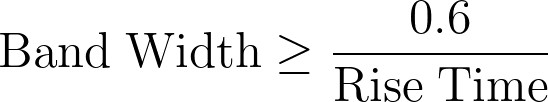
For example, a 300 ps signal would require a scope with a 2 GHz bandwidth, and a 1 GHz scope could capture at most a 600 ps signal. Please keep in mind this equation is a “back-of-an-envelope” estimation. To truly determine your needs, you’ll need to know the measurement accuracy required, the frequency response of your scope, the resistance and capacitance of your scope probes, and a few other things. It’s best to just get a test-equipment representative on the phone and explain your requirements and let them tell you which test instruments they have that can meet your needs.
If you don’t have sufficient sampling points, you won’t be able to capture the actual rise and fall times of your signal.
What does that look like in real life? Let’s take a moment to look at some actual sampled signals from a ~40 ps rise-time source on a Tektronix MDO3104 oscilloscope with a rated combined bandwidth of 1 Gsps. The Rule-Of-Thumb provided earlier says that this scope would, at best, be able to see a 600 ps rise time, a difference from the datasheet’s stated rise time by over an order-of-magnitude.
First, I set the scope for 250 MHz — as would be the maximum bandwidth on a single channel if all four channels were in use. There we see a signal that’s pretty similar to the first image that appeared in this article. It looks remarkably clean, so you might be tempted to think everything worked out as it should, write down the number, and move on. But don’t be bamboozled!
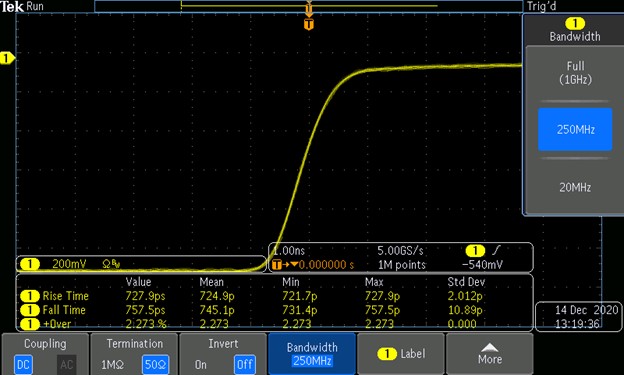
This MDO3104 oscilloscope image shows the 40 ps signal recorded with a 250 MHz bandwidth. The curve has a measured rise-time of approximately 725 ps.
Now let’s find out what that signal looks like when the entire 1 GHz bandwidth is used and the sampling increases by a factor of four.

This oscilloscope image shows the 40 ps signal recorded with a 250 MHz bandwidth. The curve has a measured rise-time of approximately 260 ps.
That’s a different signal entirely. And the measured rise time is significantly higher than before as well. We’re not seeing the true rise time of the signal — we’re seeing the limitations of the oscilloscope’s sampling rate.
This image isn’t the true representation of the signal either! We’re closer to the truth, but even though we’ve quadrupled the number of sampling points, there still aren’t enough sampled points to accurately capture and reproduce the waveform.
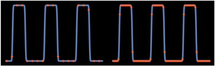
As an example, the blue signal is sampled by ~20 evenly spaced points on the left and 4x that number on the right. But as you can see, the rise and fall of the signal are not accurately sampled.
In short — for high speed signals, you need quality test equipment in your lab to truly understand what is happening to the signals in your circuits.
Simulation
Before you ever power on your test equipment or send your artwork to your fab house, you should have a thorough understanding of what is happening in your design. For that you need to find a simulation software suite that fits your requirements and your budget.
Your simulation needs will again depend on the rise-time of your devices. There are a variety of software options out there that fill numerous needs. The following list is non-exhaustive and inclusion does not mean that Royal Circuits recommends or endorses the software.
Polar Instruments PCB Stackup, Signal Integrity, and Controlled Impedance Calculators
PCB signal integrity, stackup and controlled impedance software by Polar Instruments
This software is relatively well known amongst high-speed design engineers. While it is primarily a 2D field solver, that can usually be enough for many designs.

Ansys HFSS and SIWave
RF and Microwave Simulation software from Ansys.
Ansys has multi-physics capable solvers for electromagnetic, thermal, and mechanical simulation of chip and board level designs. Two popular tools are HFSS (High Frequency Structure Simulator) and SIWave. HFSS provides 3D electromagnetic simulation for antennas, high speed interconnects, filters, etc… SIWave provides power integrity, signal integrity, and EMI analysis. It can determine power noise margins and electromagnetic compliance.
Simberian
Simberian’s Simbeor Electromagnetic Signal Integrity Software provides full 3D-wave analysis of PCB interconnects. It allows engineers to visualize and calculate cross-talk,

Summary
You need the right tools to do your job. You can either ask purchasing to make a one-time investment in better equipment, or let them know that they will have to pay for higher-grade dielectrics, repeatedly, every time a new panel or a new design is produced. And every time a board doesn’t work because you can’t accurately measure the signal.
Good luck!