PCB Fabrication Basics: How Traces Are Made

Etch Progression

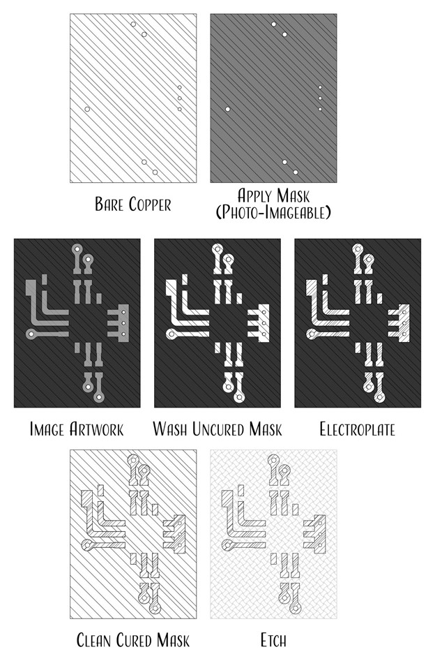
Copper foil does not etch right angles to a board surface.  Initially, only the exposed copper surfaces react and are washed away by the etchant, largely dissolving material perpendicular to the board surface.  Then, as the etchant progresses from the etch resist layer to the substrate layer, there is increased opportunity for lateral material removal.  After some time in the etching tanks, liquid etchant removes copper both perpendicular and parallel to the board surface.

At the early stages of the etching process, cross-sections of unprotected copper surfaces appear circular, and then trapezoidal with curved legs, and after extended etching, the sides may appear almost vertical.

The progression from curved to vertical requires extra time in the etch tanks and the removal of larger-than-normal amounts of copper.  Fabricators do not over-etch traces to the point of verticality unless it is specifically requested by a PCB designer.

Copper Etch Compensation

After etching, the copper closest to the etch-resist layer is generally narrower than the copper nearest the substrate layer.  To ensure adequate copper width after etching, fabrication houses must adjust copper artwork before fabrication in a process called etch compensation.  Based on the copper weight, fabricators will expand copper features into available space by 1-8 mils, so that after etching, the width of the trace meets a specified minimum. 

Copper Cut Back and Compensation

Closely packed copper features can interfere with this compensation process.  Enough room must exist between copper features to allow the etchant to move freely into an area and copper atoms to move out.  To allow adequate etch compensation on critical features, fabricators will sometimes trim the copper away from other nets in a cut-back process.

The Process

After through-holes are drilled in a panel, copper foil is covered with a photo-imageable etch resist liquid or dry-film mask and then exposed to light in a negative 1:1 pattern of the layer artwork.  The light causes chemicals in the mask to polymerize and harden.  The unpolymerized mask is washed away and the panel is then attached to the cathode of a pulsed DC power supply and submerged in electroplating tanks where copper accumulates on the exposed copper.  The remaining solder mask is then removed from the panel. 


At this point the copper foil is thicker in the parts of the board that will eventually be traces, copper pours, etc…  In the last step, the entire panel is etched — copper is removed from the entire board.  The thinner, un-plated areas of copper etch completely away before the thicker electroplated foil, so after etching, the traces and the copper pours are left behind.

There are a few more details to the process that were not discussed here, such as via fill, electroless catalysts, and more.  To learn more, contact sales@royalcircuits.com.

Recent Posts

Summit Interconnect Acquires Royal Circuit Solutions and Affiliates

The combination solidifies Summit’s position as one of the largest privately owned printed circuit board (PCB) manufacturers in North America with a  footprint that will now encompass eight manufacturing facilities. The acquisition significantly broadens the scope of Summit’s product offering while expanding the company’s business portfolio of key customers and end-markets. Summit Interconnect is pleased… View Article
Read More

Tech Chat with Thermal Expert, Mike Jouppi

Ever wondered how many vias to use in a thermal package? Or how to route high current traces in small spaces? Good news! Mike Jouppi is back! Check back for a recording of this important PCB resource. In the meantime, feel free to download the Thermal Resistance calculator discussed live.  Download Thermal Resistance Calculator
Read More

Flex PCBS: Design Tips and Material Selection Advice – On-Demand Webinar

In today’s high-tech world, electrical engineers have many choices when it comes to designing their PCBs, including what type of laminate to use. Laminates form the foundation for a high-functioning PCB. In this on-demand webinar, learn how to select the right laminate for your project based on material properties, suppliers, types and more.
Read More

Share

Share on twitter
Share on pinterest
Share on facebook
Or use this public share link