The majority of printed circuit boards made today are produced in batches on standardized panels. If you are trying to minimize the cost of your next design, you should consider your board shape and size.
While some manufacturers will make one-off boards out of material as small as 6” x 6”, all manufacturers can make panels that are nominally 18” x 24”, with either a 0.5” or 1.0” margin that is used for fixtures, fiducials, and test coupons. That leaves 16” x 22” (or 17” x 23”) of board space for your next design.
But before you go hog-wild with your next design, you need to keep a few things in mind.
Depanelization
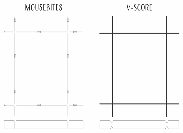
To individualize your boards from the panel, there are two general options in wide use. The first is routing, and the second is scoring. Routing leaves tiny mouse-bites in the board, and scoring cuts a 30-60° path through ⅔ of your board. Laser depanelization is available, but is expensive and not discussed here.

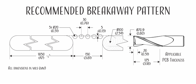
You can have your fabricator create your panel for you (preferred). Or you can create the patterns yourself. Something to keep in mind is that the end-mills used in routers only cut well in one direction, so for clean boards, you’ll need a route-path that is wider than your fabricator’s end-mill diameter.


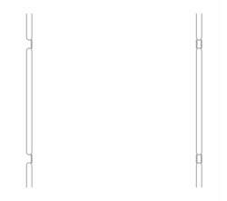
You can use single or double-sided mousebite patterns on your designs to remove the tabs on both sides of the breakaway point.
Avoid Spontaneous Depanelization and Destructive Depanelization
Something to keep in mind whether you use mouse-bites or v-scores is that the boards need to stay in the panel until it is time to remove them. If you make your boards too weak, they can spontaneously disassembly during shipping.
One way to achieve this is with skip-scoring or carefully designed routing patterns. If you create a design that stays strong until the board margins are broken away, you’ll be in great shape.

Straight Line Breaks
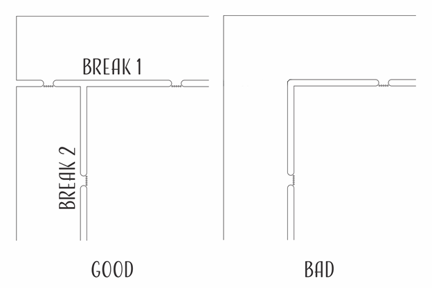
Your assembly house should only ever break in straight lines. Doing anything else can put a great deal of stress on your board — something that can damage the laminates and cause your parts to pop off the board.

Hope this helps! If you have any further questions, contact our engineering experts for more information.


