Build a Better Via Stack

Build a better via stack by thinking about how your board is assembled.

Cap vs. Foil Construction

Printed Wiring Boards are constructed in one of two ways described as “Cap” or “Foil” construction.  The construction method determines via layer options and lamination cycles.

Foil Construction

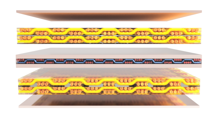
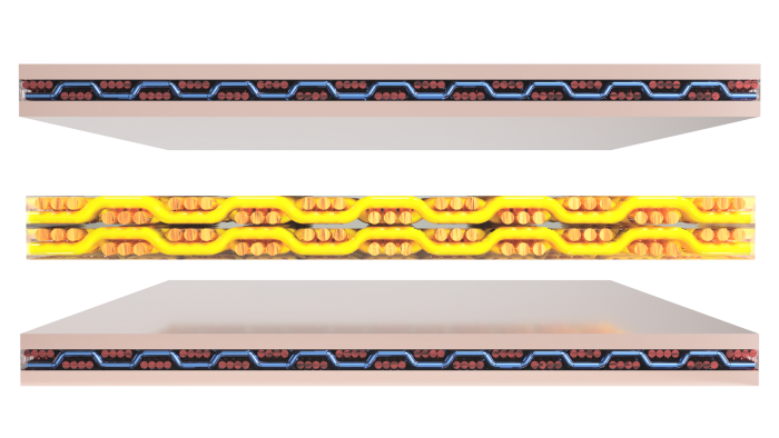
In foil construction, fabricators start by drilling, electroplating, and etching a copper-clad core that will become the innermost layer of the design.  Then additional layers of prepreg and copper are laminated to the outside of that core, and the new layers are drilled, electroplated, and etched.  The process repeats until all layers of the board have been added, usually maxing out at 18-24 layers.  After the last lamination, the board will be drilled, electroplated, and etched to create through-hole vias. 


Very high layer count boards, such as a 96-layer board used for a new microcontroller validation, can be created by combining smaller layer stacks.

In this image, a central copper-clad core (Layers 2 and 3) is layered with prepreg and copper foil (Layers 1 and 4) to create the final 4-layer stackup.

Microvias might be added to connect layers 1 and 2 or layers 3 and 4.  To connect layers 1 and 3, a designer might create a through-hole via from layers 2 to 3 and then add a staggered microvia from layer 1 to 2.  A through-hole via can be added after all layers are laminated.

Cap Construction

In Cap Construction, multiple copper-clad cores are drilled, electroplated, etched, and then laminated.  If no blind or buried vias are needed to connect the cores, multiple cores can be joined in a single lamination cycle.

In this image of a 4-layer board, blind vias can join layers 1-2 and 3-4, and a through-hole via can pass through all layers of the stack.

What does it take to make a via?

Mechanical Vias

After multiple layers of copper and dielectric material have been laminated in a hot-oil press, a high-precision drill pierces the complete-assembly or the sub-assembly in all the locations that will eventually become mechanical vias.  Next, the panel is placed in a dry-film laminator and a negative-image of the layer artwork is projected on the film, curing it and causing it to adhere to the copper underneath.  Then the uncured dry film is removed, leaving exposed copper in all areas that will eventually become traces, copper pours, and vias.  The panel then enters an electroplating bath, where copper fills in the via barrels and thickens all exposed copper.  Finally, the entire board is etched, which removes all of the unplated copper, and a small amount of the plated copper.

All mechanical (buried, blind, and through-hole) vias are formed in this manner.  Buried and blind vias only take their names after additional lamination cycles.

Microvias

Microvias are usually created to join one layer to the next in a foil-construction.  Under certain circumstances, a microvia can span two layers, but typically, the microvias would be built up one layer at a time in either a stacked or a staggered assembly.

Microvia holes are created with lasers that pierce through the topmost layer of copper and the underlying dielectric material.  The combined thickness of the dielectric and copper is equal to the minimum allowable via diameter.

Microvias may be filled in a variety of ways, but electroplated copper is the most common option.

Why do you need to know all of this?

Once you know the basic processes required to make your board, you can determine whether or not the vias that you’ve specified can actually be formed in your PCB.  Then you can start saving money in your next design by minimizing the number of lamination and via formation cycles.

Recent Posts

Summit Interconnect Acquires Royal Circuit Solutions and Affiliates

The combination solidifies Summit’s position as one of the largest privately owned printed circuit board (PCB) manufacturers in North America with a  footprint that will now encompass eight manufacturing facilities. The acquisition significantly broadens the scope of Summit’s product offering while expanding the company’s business portfolio of key customers and end-markets. Summit Interconnect is pleased… View Article
Read More

Tech Chat with Thermal Expert, Mike Jouppi

Ever wondered how many vias to use in a thermal package? Or how to route high current traces in small spaces? Good news! Mike Jouppi is back! Check back for a recording of this important PCB resource. In the meantime, feel free to download the Thermal Resistance calculator discussed live.  Download Thermal Resistance Calculator
Read More

Flex PCBS: Design Tips and Material Selection Advice – On-Demand Webinar

In today’s high-tech world, electrical engineers have many choices when it comes to designing their PCBs, including what type of laminate to use. Laminates form the foundation for a high-functioning PCB. In this on-demand webinar, learn how to select the right laminate for your project based on material properties, suppliers, types and more.
Read More

Share

Share on twitter
Share on pinterest
Share on facebook
Or use this public share link