Circuit Analysis – Part 2: Data Bus Overview

Before you layout a circuit, it’s generally a good idea to understand what is happening in your schematic.  And before you lay out a schematic, it’s generally a good idea to understand what is happening in your block diagram.

For additional information on circuit analysis, read our previous post: Circuit Analysis – Part 1: Power System Overview.

Communication Protocols

Serial data moves through a circuit from source to destination as a series of changing voltages. The sender(s) initiates the change on the signal line and the receiver detects that the potential has changed.

There are a variety of protocols that are in common use in the industry: ATA, SCSI, CAN, I²C, SPI, UART, RS232, RS485, USB, Ethernet, Microwire, 1-wire, etc… But commercial sensors predominantly use I²C and SPI.

Synchronous
Synchronous communication requires a minimum of two signal lines: one line transfers data, the other transfers the clock signal. 

Asynchronous
Asynchronous communication requires a minimum of one signal line. However, the clock frequency must be agreed to by both the sender and receiver before communication can be successful. 

I²C

The Real-Time Clock, BNO055, and BME280 all communicate with the ATMega328 via I²C.

The Inter-Integrated Circuit (I2C or I²C) protocol uses two data lines: clock and data.  The Serial Clock Line (SCL) transmits the timing information while the Serial DAta line (SDA) transmits the bits of data.  Either the master or the slave can trigger the data line, but only the master controls the clock.  This allows for half-duplex communication between master and slave.

This animation of an I2C transaction is courtesy AllAboutCircuits.com
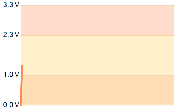
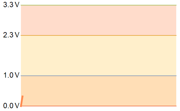
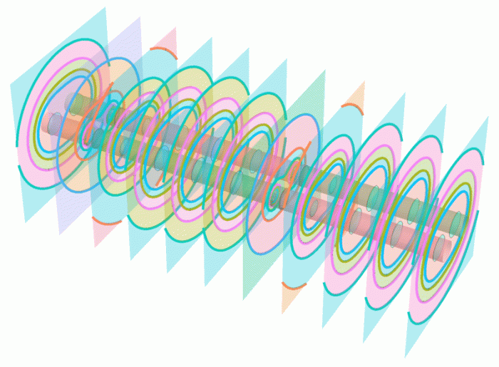
A major misconception perpetuated by textbooks is the use of ideal square-waves in all design examples. These square waves are easy for authors to draw, but do not force students to think about the real-world effects of noise and impedance on signal propagation. Real circuits never have perfectly square edges. Noise, changes in impedance, cross-talk, etc... all keep the "square-waves" drawn in textbooks from ever appearing "square" in an actual circuit.
Mark Hughes
Royal Circuits Research Analyst

Advantages
One of the advantages of the I²C protocol is that it is a multi-master, multi-slave protocol. Several microcontrollers can be on a bus and read the same sensor data, provided they aren’t both controlling the clock signal at the same time. Usually, I²C is used by a single microcontroller to communicate with several slaves, such as EEPROM, sensors, displays, etc…

Disadvantages
Address Collisions
Many of the devices on the I²C bus have 7-bit addresses. With only <128 possible addresses (2^7=128, but not all addresses are used), it’s entirely possible to select two devices with identical addresses. Fortunately, most manufacturers provide a workaround by adding an address (ADDR) or multipurpose (MP) pin to their design that allows designers to change the address by changing the logic level of a pin.

Capacitance
A second disadvantage is that high bus capacitance negatively impacts the maximum data rate. The I²C bus is meant for relatively slow, short-distance communication on a single board. While it can sometimes tolerate transmission via discrete wire connections to other boards, it is not designed for that purpose, especially at high speeds.

I²C Engineering Considerations

I²C master devices will pull the logic-signal directly to ground potential, and allow the pull-up resistors to bring the logic levels to Vcc potential.  The logic-high to logic-low transition is fast and looks quite a bit like a square-waveform on an oscilloscope.  But the logic-low to logic-high transition is mediated by the bus capacitance and the selection of pull-up resistors.

In the case of the I²C example, the RC-constant of the logic-high transition is the limiting factor in bus-speed.  The resistance is provided largely by two pull-up resistors as well as a minor amount of trace resistance.  The capacitance is the sum of trace capacitance, pin capacitance, and any other stray capacitance along the signal path.  The I2C specification limits the maximum capacitance to 400 pF for standard (100 kHz) and fast mode (400 kHz), and 500 pF for fast mode plus (1 MHz). 400 pF is not a lot of capacitance.  An individual I/O pin might have a capacitance of 2-10 pF, and a 6 mil trace increases capacitance by a little less than 2 pF/inch in FR-4 material above a ground plane. 

Binary Logic

Binary logic has two states: high and low.  The logic high state of an integrated circuit might be any potential difference between 70% and 100% of Vcc, and the logic low state is often any potential difference between 0 and 30% of Vcc.  In between 30% and 70% the logic is undefined.  (These aren’t the only logic thresholds, but are a good starting point for explanation sake.)

This is a slightly more realistic I2C clock signal. Image courtesy AllAboutCircuits.com

When the bus capacitance gets too high, the rising signal is unable to reach the logic-high state before the master device’s logic-state changes and the signal falls back into a logic-low state.  

his image shows the effects of too much capacitance and too much resistance which prevents the signal from ever reaching a logic-high state. Image courtesy AllAboutCircuits.com

Resistor Selection

To ensure that the signals reach the logic-high state in time, you should use a low-value pull-up resistor.  But if the resistor value is too low, you risk running too much current through your microcontroller, and you will dissipate a great deal of energy every time you run an I²C transaction.  Ideally, you will calculate the value of your pull up resistor based on the bus-capacitance and the I²C mode rise-time (standard, fast, or fast-mode plus). 

Remember to choose a resistor in the E-24 series to keep costs down. 

The minimum resistor is much easier to calculate.  The pins on your master and slave devices have maximum source/sink specifications listed in their datasheets.  Find the lowest-value sink specification and use Ohm’s law to calculate the minimum resistance.

SPI

The ATMega328 communicates with the display through the SPI bus.

The Serial Peripheral Interface (SPI) is a bi-directional, synchronous data transfer protocol.  This protocol requires at least three data lines, Master In Slave Out (MISO), Master Out Slave In (MOSI), and Clock (CLK).  An optional data line called Slave Select Not ( SS) is used to enable or disable data transmission on one or many integrated circuits.  The overline indicates that the logic for this digital input is inverted:  slave select is active, and a chip is enabled, when the logic is low.  In many designs, this digital input can be tied to the ground net to permanently enable the data bus.

This image shows the Daisy-Chain configuration where data is passed from one microcontroller to the next. A multiple-slave select option is also available. Image courtesy AllAboutCircuits.com

Data that is stored in a linear shift register is moved over bit by bit with each clock cycle.  SPI is a full-duplex protocol — the sender and receiver can both transfer data at the same time.

If you were to watch the signals transition on an oscilloscope — you would see data on both the MOSI and the MISO lines.

SPI Transaction courtesy AllAboutCircuits.com

USB

The Universal Serial Bus specification relies on differential pair signaling to transfer data along its length at high speeds. A differential pair consists of two digital signal lines that have the same amplitude but opposite polarity. Our circuit does not necessarily require special handling of the differential pair signals, but we will talk about them nonetheless. And since this is not a course on signal integrity, I’ll spare you the physics for now. But feel free to ask questions in the forums.

Design Rules

For a differential pair to work as intended, the individual traces need to have consistent width and have consistent spacing to other conductors, and the two traces should remain as identical as possible — following an identical path and have identical length. The general idea is that a Low→High transition needs to propagate along the wire parallel to and at the same time as a High→Low transition. The electric fields are confined tightly between the two traces if the two signals travel the same distance over the same dielectric.

This animation shows the electric fields surrounding two opposite polarity pulses (red and green cylinders) moving through two parallel wires. As long as the opposite polarity pulses are timed properly, the electric fields remain tightly confined to the area around the wires. (Similar graphics at AllAboutCircuits.com)

If the traces/wires are not the same lengths, or if the impedance changes in the surrounding environment, the symmetry between the two wires is lost, and one transition will lead or lag the other.  When the two wires have the same polarity, the electric fields repel and can spread further from the wires.

This animation shows the electric fields surrounding two similar polarity pulses (red and green cylinders) moving through two parallel wires. The electric field lines here are repulsive.

Electromagnetic interference is the result of rapidly changing electromagnetic fields.  If the field lines in the first animation switch to look like the second animation, or back again, the electromagnetic field disturbance will propagate outwards from your traces to other areas of your circuit, or into the broader environment.

So the purpose of differential-pair routing is to ensure that the two wires stay as symmetric as possible over as equal a distance and as short a distance as possible.

UART

The Universal Asynchronous Receive and Transmit protocol allows full-duplex communication between two nodes.  The only requirement is that the two nodes agree upon a common transmission rate (BAUD rate).

Unlike the other communication protocols used in our design, UART requires a cross-over connection. Transmit→Receive and Receive→Transmit. 

Uart Connection from CircuitBasics.com shows a cross-over connection between the two ICs.

Since it has a relatively slow transmission rate, UART data lines can run the full length of an entire PCB panel and off-board through several meters of wiring without much an issue.

Asynchronous communication nodes are usually tolerant of a slight timing mismatch.  But if the transmission rates are too different than receiving rates, the information ends up garbled.  If you ever see random characters or no characters on a serial-debug screen, the usual culprit is a timing mismatch.  

In next week’s blog post on circuit analysis we discuss sensors, clocks and switches. 

Recent Posts

Summit Interconnect Acquires Royal Circuit Solutions and Affiliates

The combination solidifies Summit’s position as one of the largest privately owned printed circuit board (PCB) manufacturers in North America with a  footprint that will now encompass eight manufacturing facilities. The acquisition significantly broadens the scope of Summit’s product offering while expanding the company’s business portfolio of key customers and end-markets. Summit Interconnect is pleased… View Article
Read More

Tech Chat with Thermal Expert, Mike Jouppi

Ever wondered how many vias to use in a thermal package? Or how to route high current traces in small spaces? Good news! Mike Jouppi is back! Check back for a recording of this important PCB resource. In the meantime, feel free to download the Thermal Resistance calculator discussed live.  Download Thermal Resistance Calculator
Read More

Flex PCBS: Design Tips and Material Selection Advice – On-Demand Webinar

In today’s high-tech world, electrical engineers have many choices when it comes to designing their PCBs, including what type of laminate to use. Laminates form the foundation for a high-functioning PCB. In this on-demand webinar, learn how to select the right laminate for your project based on material properties, suppliers, types and more.
Read More

Share

Share on twitter
Share on pinterest
Share on facebook
Or use this public share link