The 4 Basic Parts of Every EDA Tool

Every Electronic Design Automation (EDA) tool is a bit different.  Some have more features than others, some have different features, some offer simulation, some don’t.  But they all have a few features in common: they allow designers to capture a schematic and layout a PCB.

In a schematic diagram, components are represented as abstract symbols.  

Schematic symbols by Filip Dominec from Wikipedia.org.

On a printed circuit board, components are attached to copper pads arranged in carefully designed land patterns.

Image of land patterns from practicalcomponents.com

To create a design, you need a part library that has all of your components’ land patterns associated with the components’ schematic representation.

Basic EDA Structure

There are four basic parts of every EDA tool.  The pattern editor, component editor, schematic layout, and PCB layout program.  The names of the modules might vary from program to program, and they might be used differently, but they all exist in one form or another. 

  • Component editors alter the appearance of schematic symbols.
  • Pattern editors alter the appearance of land patterns.
  • Libraries hold collections of linked components and patterns for reuse from design to design.
  • Schematic Layout arranges the connections between components.
  • PCB Layout arranges the patterns and the traces that connect them.

Libraries hold groups of footprints and components.  When a component is selected for use in a schematic, it’s associated land pattern is prepared for use in the PCB layout portion of the software.

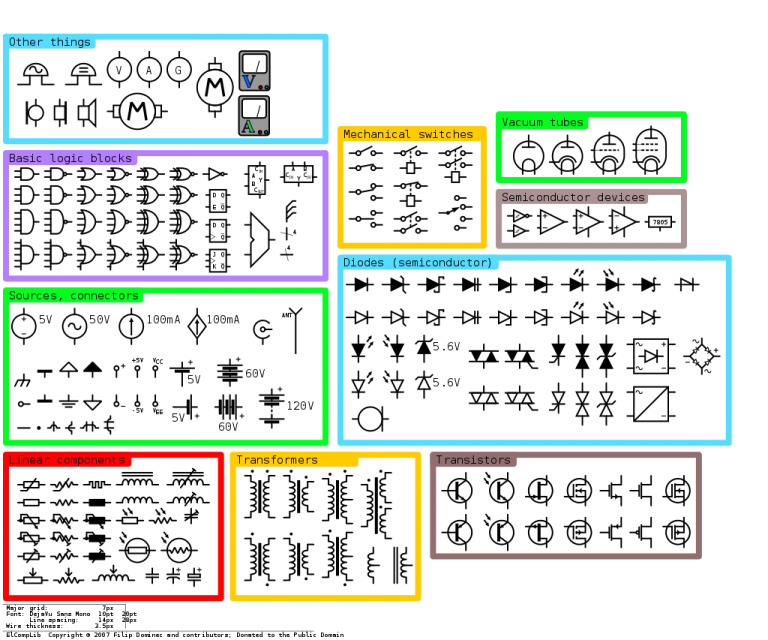
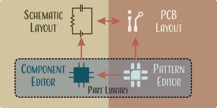
I have never worked in any version of any EDA program that had a complete, up-to-date, and accurate parts library. I've always had to add several components of my own. Sometimes the libraries are so bad, I've added all of my own parts. Creating custom libraries and ensuring their accuracy is probably the most time-consuming and tedious aspect of any design. If you don't enjoy managing your own parts libraries, services such as PCBLayout.com and Octopart's eConcierge service will manage your libraries for you.
Mark Hughes
Research Analyst

Pattern Editor

Engineers use the term footprint to describe the outline of the bottom of a discrete component and its pads/pins

This bottom-side view of a QFN28 package shows the metalized pads that will be soldered to a landing pattern (not shown).
This artistic image of a 14TSSOP package hovering over a matching land pattern. Notice that the lands are larger than the gull-wing pins, but both are equally spaced.

To make things even more exciting/confusing, the land patterns associated with those pads are often incorrectly called footprints by engineers, even though the metalized lands have to be larger than the metalized pads/pins they mate with.  Electronics Engineering is terrifically confusing to begin with, the situation is not improved by engineers that use the same words to describe two different things.  But that’s the world we live in, so let’s try to make sense of it.

  • Discrete components have metalized pads or pins on their base and sides. 
  • Printed circuit boards have metalized lands on their outer layers. 

These two metalized parts have a similar pattern but are two different sizes.  Solder connects the lands to the pads/pins

For a proper solder joint to form, the solder has to form a filet, and the only way that can happen is if the land is bigger than the pad/pin

A discrete component’s metalized pad pattern and a printed circuit board’s land pattern are identical in layout and centerline spacing, but the metalized lands are always bigger than the metalized pads.

The size and shape of footprints and lands has been largely standardized into IPC-7351, a document that describes the pin pattern, layout, and naming convention for all standard parts.  The document is unfortunately locked behind a paywall.  That’s okay, it’s not a very exciting read, and most EDA programs have incorporated the data from the document into their pattern editor libraries.  “Wizards” generate the pattern and pattern names needed in the program.  Additional patterns can be constructed manually from information supplied in datasheets.

Component Editor

The abstract symbols that represent PCB components are created and edited in a component editor.  Components are shapes that abstractly define the function of a physical part, with pins that represent metalized pads/pins on physical components.  There are two standards in broad use and as long as the symbols don’t jump from one standard to another within a schematic document, it’s usually pretty easy to keep track of what is going on.

Schematic Capture

Schematic Capture is the part of the program that takes the components from the library and lays them out on a document.  Parts are connected with virtual wires that allow designers to see the electrical connections between pins.  A set of pins that are electrically connected is called a net.

A schematic representation of a Hartley oscillator

When you pull a component from the library, you should do two things.

  1. Make sure the part is available.  It’s very common for EDA part libraries to be out of date and include parts that are now obsolete and unobtainable.
  2. Double-check the land pattern that is associated with the part number is correct.  You never know who made the library entry, and it’s possible that they read the datasheet incorrectly or they copied the footprint in a 1:1 manner.

Electronics design and layout is a complicated activity.  So engineers often take shortcuts where they can find them.  It’s quite common for a designer to have a “grab-bag” of sub-circuits that, once proven successful, they will reuse from design to design.  There’s no need to redesign everything from scratch every time.

Top-Down Design

At the beginning of the course, Bob and I had a phone call where we talked about what design elements we wanted to include in the badge (IMU – Yes, Neopixel – Yes, Wireless – No, etc…).  Then we drew a block diagram.  At that point, Bob started designing each of the blocks as a separate circuit.

This is one of the early block diagrams -- things didn't change very much in the months that followed.

The current schematic was born out of each one of those blocks.  With a top-level block that shows the connections between all of the various sub-circuits.

ou should go through a careful schematic review process before you move on to layout.  Even the simplest schematic is complicated.  Errors caught at the schematic stage can save hours of rework at the layout stage.

PCB Layout

While you have been layout out your schematic, your EDA has been quietly been keeping track of your land patterns, and the connections between the pins.  If it’s been set up properly, there’s a good chance that it knows which pins require special routing rules as well.

But when you first convert it, you usually get an explosion of parts onto a blank page connected with a flurry of ratlines.

At that point, it’s usually a good idea to remove the ratlines from view and organize the parts by circuit block.

At that point, you can start positioning the parts on the PCB and running traces to connect them.

This article is part of the course content on Rigid PCBs at TeachMePCB.com  Sign up for our next course now!

Recent Posts

Summit Interconnect Acquires Royal Circuit Solutions and Affiliates

The combination solidifies Summit’s position as one of the largest privately owned printed circuit board (PCB) manufacturers in North America with a  footprint that will now encompass eight manufacturing facilities. The acquisition significantly broadens the scope of Summit’s product offering while expanding the company’s business portfolio of key customers and end-markets. Summit Interconnect is pleased… View Article
Read More

Tech Chat with Thermal Expert, Mike Jouppi

Ever wondered how many vias to use in a thermal package? Or how to route high current traces in small spaces? Good news! Mike Jouppi is back! Check back for a recording of this important PCB resource. In the meantime, feel free to download the Thermal Resistance calculator discussed live.  Download Thermal Resistance Calculator
Read More

Flex PCBS: Design Tips and Material Selection Advice – On-Demand Webinar

In today’s high-tech world, electrical engineers have many choices when it comes to designing their PCBs, including what type of laminate to use. Laminates form the foundation for a high-functioning PCB. In this on-demand webinar, learn how to select the right laminate for your project based on material properties, suppliers, types and more.
Read More

Share

Share on twitter
Share on pinterest
Share on facebook
Or use this public share link