PCB Design Rules

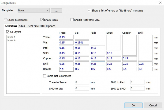
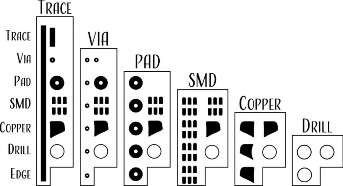
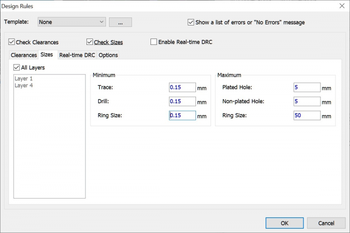
Every fabrication shop has a list of design rules that they provide to customers that detail the limitations of the manufacturing process.  The specific numbers used will depend on the fabrication shop that you use as well as whether you are using their recommended process limits or their actual process limits.  Remember that the closer that you get to the actual process limits, the more expensive your design will be to produce.  Included in the rules are distances between traces, board edges, pads, etc… 

Space Width

You set the spacing between copper features in your design program and then have the software check your PCB layout against the numbers.  This is the “Space Width” part of Trace and Space width.  Remember that different copper weights have different trace and space minimums, so if you have thicker inner layers of copper, you’ll want to provide separate rules for those layers.

Example of Design Rules Copper Space clearances from DipTrace

All of these values reference the minimum distance between two PCB features.  Remember that PCB fabrication has some imperfections associated with it.  If you take everything to the absolute manufacturing limits, then your board yield per panel will decrease.

The matrix above compares the minimum spacing of objects in your design. In Diptrace, Pad refers to a through-hole pad and SMD refers to a surface mount pad.

Notes:

  • Most of the values in the trace/space charts are limited by manufacturing minimums associated with copper weight. You might consider making templates based on common copper weights (0.5 oz, 1 oz, 1.5 oz, 2 oz, etc…) and then simply assign the template to each layer of your design based on your stackup.
  • Metric and Imperial measurements don’t often convert well in the various EDA programs. Since layout is most often done in metric measurements, you might consider metric layout rules.
  • You might consider giving yourself a “fudge-factor” when setting up clearances. Some round shapes such as copper pour fillets, spirals, circles, etc… will be converted into straight-line segments or polygons by your EDA program. The straight-line segments that make up the line will move towards other features on the concave side of the curve — this creates DFM errors — by using numbers a few percents higher than manufacturer recommendations, you can avoid this problem. Better yet, give your self a few additional mils clearance whenever possible.
This spiral is made of intersecting semi-circular segments of arithmetically increasing radii. Some EDA programs will replace spirals with straight-line segments in gerber files.

Trace Width

Copper clearance isn’t the only concern.  You also need to ensure that your minimum copper trace widths are met, there is a minimum size drill hole, minimum annular ring, etc…  These are determined by the minimums provided by your design house.

Example of Design Rules Copper Widths from DipTrace.

Recent Posts

Summit Interconnect Acquires Royal Circuit Solutions and Affiliates

The combination solidifies Summit’s position as one of the largest privately owned printed circuit board (PCB) manufacturers in North America with a  footprint that will now encompass eight manufacturing facilities. The acquisition significantly broadens the scope of Summit’s product offering while expanding the company’s business portfolio of key customers and end-markets. Summit Interconnect is pleased… View Article
Read More

Tech Chat with Thermal Expert, Mike Jouppi

Ever wondered how many vias to use in a thermal package? Or how to route high current traces in small spaces? Good news! Mike Jouppi is back! Check back for a recording of this important PCB resource. In the meantime, feel free to download the Thermal Resistance calculator discussed live.  Download Thermal Resistance Calculator
Read More

Flex PCBS: Design Tips and Material Selection Advice – On-Demand Webinar

In today’s high-tech world, electrical engineers have many choices when it comes to designing their PCBs, including what type of laminate to use. Laminates form the foundation for a high-functioning PCB. In this on-demand webinar, learn how to select the right laminate for your project based on material properties, suppliers, types and more.
Read More

Share

Share on twitter
Share on pinterest
Share on facebook
Or use this public share link