Copper Trace and Space: Three Factors to Consider

When it comes to creating printed circuit boards, engineers often guestimate various aspects of their design. One such design metric is known colloquially as Trace and SpaceTrace refers to the width of a particular copper track, and Space refers to the width of the gap between two adjacent pieces of copper.

The trace and space are based on a variety of factors. This paper provides basic instructions on how to determine appropriate trace and space guidelines. An appendix to this document provides engineers a variety of design guidelines and graphs that will help them estimate appropriate trace and space widths.

The green trace shown here has an 8 mil trace width. It is separated from other nets by 8 mils of space between nets. This is not an impedance-controlled net and the manufacturing minimums for the board shop are 3.5 mils of space/trace on 0.25 oz./ft² copper, so the slight via pad incursions are of little consequence. 

Impedance Control

RF Engineers and High-Speed Digital Design engineers have to carefully route their traces (and their signal return paths) through the various layers of their boards. Dr. Eric Bogatin often states, “There are two types of Antenna Engineers: Those who know they are designing antennas, and those who don’t.” So, to keep the reflections and radiated emissions of your board low, you need a constant impedance on high-speed digital and rf nets.

Whenever a copper trace changes width, layer, or substrate, the speed of propagation changes and a portion of the signal is reflected or radiated into space. It is important that differential-pairs and single-ended high-speed digital signals are given route priority at the very beginning of your design to minimize layer transitions and traces from other nets should not cross above or below these lines unless there is a plane-layer between them.

Two sets of differential pairs, shown in blue and red are the first traces routed in this design.

Once you know you have an impedance-controlled trace on your design, you should communicate with your fabricator, who will determine the trace and space specifications you can use to route your design. The fabricators combine simulation software with real-world experience to determine the proper specifications.

This sample stackup from Royal Flex Circuits shows a 6-layer rigid-flex design stack.
The predicted impedance of the stackup is compared against test-coupons fabricated alongside the PCB.

Each layer of your design has unique material properties and can potentially require different trace and space requirements to achieve a constant impedance. If you have a 7 mil-trace with 14-mil space on an external-layer, there is very little chance that those same numbers apply to the net when you transition to an internal layer.

Temperature Control

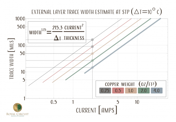
Power-design engineers are usually more concerned with their board bursting into flames than with their eye-diagrams closing. So, the question they usually ask is “How much current can I put through this trace?”. That answer was originally given in IPC-2221, which has been superseded by IPC-2152. Unfortunately, most online calculators are based on IPC-2221, which, in turn, is based on the work of two underfunded researchers from 1956 who openly admitted that they guessed appropriate derating values and never intended their work to be taken as gospel.

IPC-2152 was released five years ago and it is based on empirically determined data from this century. But the charts and graphs presented in the standards document can be far too conservative in some instances and not nearly conservative enough for exceptionally high currents. So, use them as an estimate only. All prototypes should be field-tested before going into mass-production

Drs. Douglas Brooks and Johannes Adam’s wrote a book entitled “PCB Trace and Via Currents and Temperatures: The Complete Analysis” that should be on the shelf of power-engineers. But for those of us who don’t have the book, Dr. Brooks released chapter two to all interested parties for free at his website. There, the authors found a mathematical model that fits the data presented in IPC-2152.

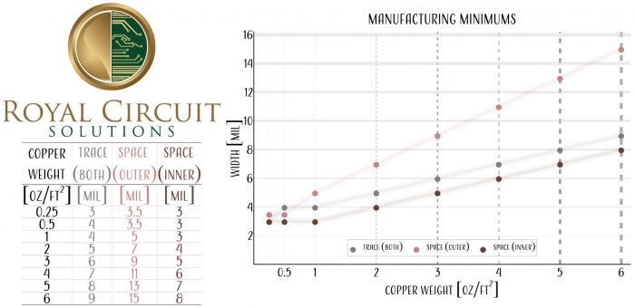
To further simplify life, Royal Circuits, in partnership with Advanced Assembly, redrew the graphs to make life easier for engineers. To be clear, the graphs provide estimates only and should not be used to make final design decisions.

The graphs indicate the minimum trace width for a given current at a variety of common copper weights. Note that the graph presented is for an external layer, at sea level and 20°C. Internal layers use a different coefficient.

To use the graph package, determine the maximum safe operating temperature for your PCB substrate, as well as the maximum expected environmental conditions of the design as well as an appropriate derating factor. Maximums are not the only consideration. The stresses caused by mis-matched coefficients of thermal-expansion play a role as well. Thermal cycling at relatively low temperatures might destroy your design long before you ever approach an upper temperature limit.

For example, perhaps you have a device that will turn on and off multiple times a day. You have chosen a laminate that has a high coefficient of thermal expansion compared to copper. It is best to limit the allowable temperature fluctuation to reduce the tensile stresses caused by thermal-cycling and you decide 10°C is allowable temperature fluctuation. Next, determine the current through a given trace. For argument’s sake, assume 2 A of current. The graph shows the approximate trace width at each of five common copper weights (other available weights are not shown on the graph to reduce clutter). A 90-mil trace is needed on 0.5 oz. copper, a 50-mil trace is needed on 1-oz copper, and a measly 15-mil trace is needed on 4.0 oz. copper. Although not shown, it’s easy enough to extrapolate the data to see that 3-oz copper would require a trace somewhere between 15-mil and 25-mil.

Remember that these graphs are estimates only and are certainly no substitute for field-testing or computer simulation. But they should be useful in determining copper weight and track thickness in many cases.

Manufacturing Minimums

New engineers love to live on the edge, while graybeards do it only out of necessity. Whenever a design pushes the absolute limits of manufacturing, not every board on a panel will work. The ratio of successes to tries is known as the “yield” and controlling the yield is critical to keep the cost of your design low. So, whenever you talk to a fabrication-house, and ask them what their absolute minimum trace/space guidelines are, you should also ask them what their “preferred” minimums are as well.

Copper doesn’t etch vertically down from a mask to the substrate, it etches at an angle, so fabricators have to include etch-back compensation. Thicker copper requires a larger set-back. 

Conclusion

These are just three factors that affect your trace and space guidelines for ridgid circuit boards. Remember though, they are only guidelines. Engineers are ultimately responsible for the designs that they make. Make sure you give yourself time to test your device in the field, and if testing isn’t possible beforehand (downhole and space), be sure to use a proper multi-physics simulator.

View appendix for additional calculations. 

Recent Posts

Summit Interconnect Acquires Royal Circuit Solutions and Affiliates

The combination solidifies Summit’s position as one of the largest privately owned printed circuit board (PCB) manufacturers in North America with a  footprint that will now encompass eight manufacturing facilities. The acquisition significantly broadens the scope of Summit’s product offering while expanding the company’s business portfolio of key customers and end-markets. Summit Interconnect is pleased… View Article
Read More

Tech Chat with Thermal Expert, Mike Jouppi

Ever wondered how many vias to use in a thermal package? Or how to route high current traces in small spaces? Good news! Mike Jouppi is back! Check back for a recording of this important PCB resource. In the meantime, feel free to download the Thermal Resistance calculator discussed live.  Download Thermal Resistance Calculator
Read More

Flex PCBS: Design Tips and Material Selection Advice – On-Demand Webinar

In today’s high-tech world, electrical engineers have many choices when it comes to designing their PCBs, including what type of laminate to use. Laminates form the foundation for a high-functioning PCB. In this on-demand webinar, learn how to select the right laminate for your project based on material properties, suppliers, types and more.
Read More

Share

Share on twitter
Share on pinterest
Share on facebook
Or use this public share link